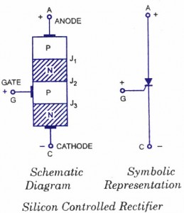
As the terminology indicates, the SCR is a controlled rectifier constructed of a silicon semiconductor material with a third terminal for control purposes. Silicon was chosen because of its high temperature and power capabilities. The basic operation of the SCR is different from that of an ordinary two-layer semiconductor diode in that a third terminal called a gate, determines when the rectifier switches from the open-circuit to short-circuit state. It is not enough simply to forward-bias the anode-to-cathode region of the device. In the conduction state the dynamic resistance of the SCR is typically 0.01 to 0.1 ohm and reverse resistance is typically 100 kilo ohm or more. It is widely used as a switching device in power control applications. It can control loads by switching on and off upto many thousand times a second. It can switch on for a variable lengths of time duration, thereby delivering desired amount of power to the load. Thus, it possesses the advantage of a rheostat as well as a switch with none of their drawback. A schematic diagram and symbolic representation of an SCR are shown in figures a & b respectively. As illustrated in fig-a, SCR is a three-terminal four-layer semiconductor device, the layers being alternately of P-type and N-type. The junctions are marked Jj, J2 and J3 (junctions Jj and J3 operate in forward direction while middle junction J2 operates in the reverse direction) whereas the three terminals are anode (A), cathode (C) and gate (G) which is connected to the inner P-type layer. The function of the gate is to control the firing of SCR. In normal operating conditions, anode is positive with respect to cathode.
Construction of an SCR
The basic material used for fabrication of an SCR is N-type silicon. It has a specific resistance of about 6 ohm-mm. Silicon is the natural choice as base material because of the following advantages
(i) ability to withstand high junction temperature of the order of 150° C
(ii) high thermal conductivity;
(iii) less variations in characteristics with temperature; and
(iv) less leakage current in P-N junction.
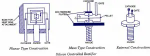
It consists, essentially, of a four layer pellet of P and N type silicon semiconductor materials. The junctions are diffused or alloyed. The material which may be used for P diffusion is aluminium and for N diffusion is phosphorous. The contact with anode can be made with an aluminium foil and through cathode and gate by metal sheet. Diffusion must be carried out at a proper temperature and for necessary duration to provide correct concentration because this decides the properties of the device. Low power SCRs employ the planar construction shown in fig a. Planar construction is useful for making a number of units from a silicon wafer. Here, all the junctions are diffused. The other technique is the mesa construction shown in fig.b. This technique is used for high power SCRs. In this technique, the inner junction J2 is obtained by diffusion, and then the outer two layers are alloyed to it. The PNPN pellet is properly braced with tungsten or molybdenum plates to provide greater mechanical strength and make it capable of handling large currents. One of these plates is hard soldered to a copper or an aluminium stud, which is threaded for attachment to a heat sink. This provides an efficient thermal path for conducting the internal losses to the surrounding medium. The uses of hard solder between the pellet and back-up plates minimises thermal fatigue, when the SCRs are subjected to temperature induced stresses. For medium and low power SCRs, the pellet is mounted directly on the copper stud or casing, using a soft solder which absorbs the thermal stresses set up by differential expansion and provides a good thermal path for heat transfer. For a larger cooling arrangement, which is required for high power SCRs, the press-pack or hockey-puck construction is employed, which provides for double-sided air for cooling.
The salient features to be considered, while designing an SCR, are the diameter and thickness of wafer, composition of the base material, type and amount of the material to be diffused into the wafer, shape, position and contact area of the gate, shape and size of the SCR, type of heat sink etc.
Fabrication technology determines various properties of the device. The voltage rating of a device can be increased by lightly doping the inner two layers and increasing their thickness. But due to this increased resistance, forward voltage drop increases and large triggering currents are required causing greater power dissipation accompanied by smaller current ratings. The heat dissipation of silicon falls from 1.5 W/cm2 at 25° C to 1.25 W/ cm2 at 125° C. A high voltage power device can seldom be used beyond 125° C.
The current carrying capacity and voltage rating of the device can be increased by irradiating silicon with neutrons. The current rating of the device can also be increased by reducing the current density at the junction but this result in a bulky device with large turn-on time.
SCR-Volt-ampere-Character
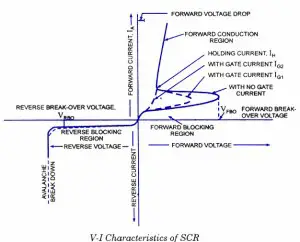
As already mentioned, the SCR is a four-layer device with three terminals, namely, the anode, the cathode and the gate. When the anode is made positive with respect to the cathode, junctions J1 and J3 are forward biased and junction J2 is reverse-biased and only the leakage current will flow through the device. The SCR is then said to be in the forward blocking state or in the forward mode or off state. But when the cathode is made positive with respect to the anode, junctions J1 and J3 are reverse-biased, a small reverse leakage current will flow through the SCR and the SGR is said to be in the reverse blocking state or in reverse mode.
When the anode is positive with respect to cathode i.e. when the SCR is in forward mode, the SCR does not conduct unless the forward voltage exceeds certain value, called the forward breakover voltage, VFB0. In non-conducting state, the current through the SCR is the leakage current which is very small and is negligible. If a positive gate current is supplied, the SCR can become conducting at a voltage much lesser than forward break-over voltage. The larger the gate current, lower the break-over voltage. With sufficiently large gate current, the SCR behaves identical to PN rectifier. Once the SCR is switched on, the forward voltage drop across it is suddenly reduced to very small value, say about 1 volt. In the conducting or on-state, the current through the SCR is limited by the external impedance.
When the anode is negative with respect to cathode, that is when the SCR is in reverse mode or in blocking state no current flows through the SCR except very small leakage current of the order of few micro-amperes. But if the reverse voltage is increased beyond a certain value, called the reverse break-over voltage, VRB0 avalanche break down takes place. Forward break-over voltage VFB0 is usually higher than reverse breakover voltage,VRBO.
From the foregoing discussion, it can be seen that the SCR has two stable and reversible operating states. The change over from off-state to on-state, called turn-on, can be achieved by increasing the forward voltage beyond VFB0. A more convenient and useful method of turn-on the device employs the gate drive. If the forward voltage is less than the forward break-over voltage, VFB0, it can be turned-on by applying a positive voltage between the gate and the cathode. This method is called the gate control. Another very important feature of the gate is that once the SCR is triggered to on-state the gate loses its control.
The switching action of gate takes place only when
(i) SCR is forward biased i.e. anode is positive with respect to cathode, and
(ii) Suitable positive voltage is applied between the gate and the cathode.
Once the SCR has been switched on, it has no control on the amount of current flowing through it. The current through the SCR is entirely controlled by the external impedance connected in the circuit and the applied voltage. There is, however, a very small, about 1 V, potential drop across the SCR. The forward current through the SCR can be reduced by reducing the applied voltage or by increasing the circuit impedance. There is, however, a minimum forward current that must be maintained to keep the SCR in conducting state. This is called the holding current rating of SCR. If the current through the SCR is reduced below the level of holding current, the device returns to off-state or blocking state.
The SCR can be switched off by reducing the forward current below the level of holding current which may be done either by reducing the applied voltage or by increasing the circuit impedance.
Note : The gate can only trigger or switch-on the SCR, it cannot switch off.
Alternatively the SCR can be switched off by applying negative voltage to the anode (reverse mode), the SCR naturally will be switched off.
Here one point is worth mentioning, the SCR takes certain time to switch off. The time, called the turn-off time, must be allowed before forward voltage may be applied again otherwise the device will switch-on with forward voltage without any gate pulse. The turn-off time is about 15 micro-seconds, which is immaterial when dealing with power frequency, but this becomes important in the inverter circuits, which are to operate at high frequency.


No comments:
Post a Comment